

Mask inspection for Extreme Ultraviolet Lithography
The technology is utilizing 13.5 nm wavelength radiation from high power plasma sources, reflective condenser optics, multilayer-coated reflective masks and all-reflective multilayer-coated aspheric objectives.
The characterization of (unstructured) mask substrates and multilayer-coated mask blanks as well as the characterization of the final (structured) reticle mask regarding possible defect sizes, defect types and locations is of major importance for the mitigation of mask defects or the final realization of near-defect-free EUVL masks.
Towards this goal, we have developed and setup (in a joint collaboration with the University of Mainz, Prof. Schönhense, and the company FOCUS GMBH, Hünstetten) an actinic (= at-wavelength) mask imaging microscope for full-sized 6 inch masks based on a micro-focused near-normal incidence illumination of the mask at 13.5 nm and an imaging Photoelectron Emission Microscope (PEEM) at the Berlin electron storage ring BESSY II.
Visualization of buried defects enhanced by standing-wave assisted actinic PEEM microscopy has been studied, allowing for the detection of sub-30 nm defects, which were invisible for non-actinic detection tools.
|
|
|
|
|
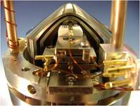
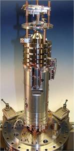
Left top and right: PEEM with temporary sample stage
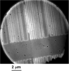
Left bottom: EUV-PEEM image of the varied-linewidth steps